Electrical Experiments with SEELab 3.0
Full wave rectifier with and without capacitor
A center-tapped full wave rectifier built with two diodes, studied with SEELab3 — first without a smoothing capacitor, then with one added across the load
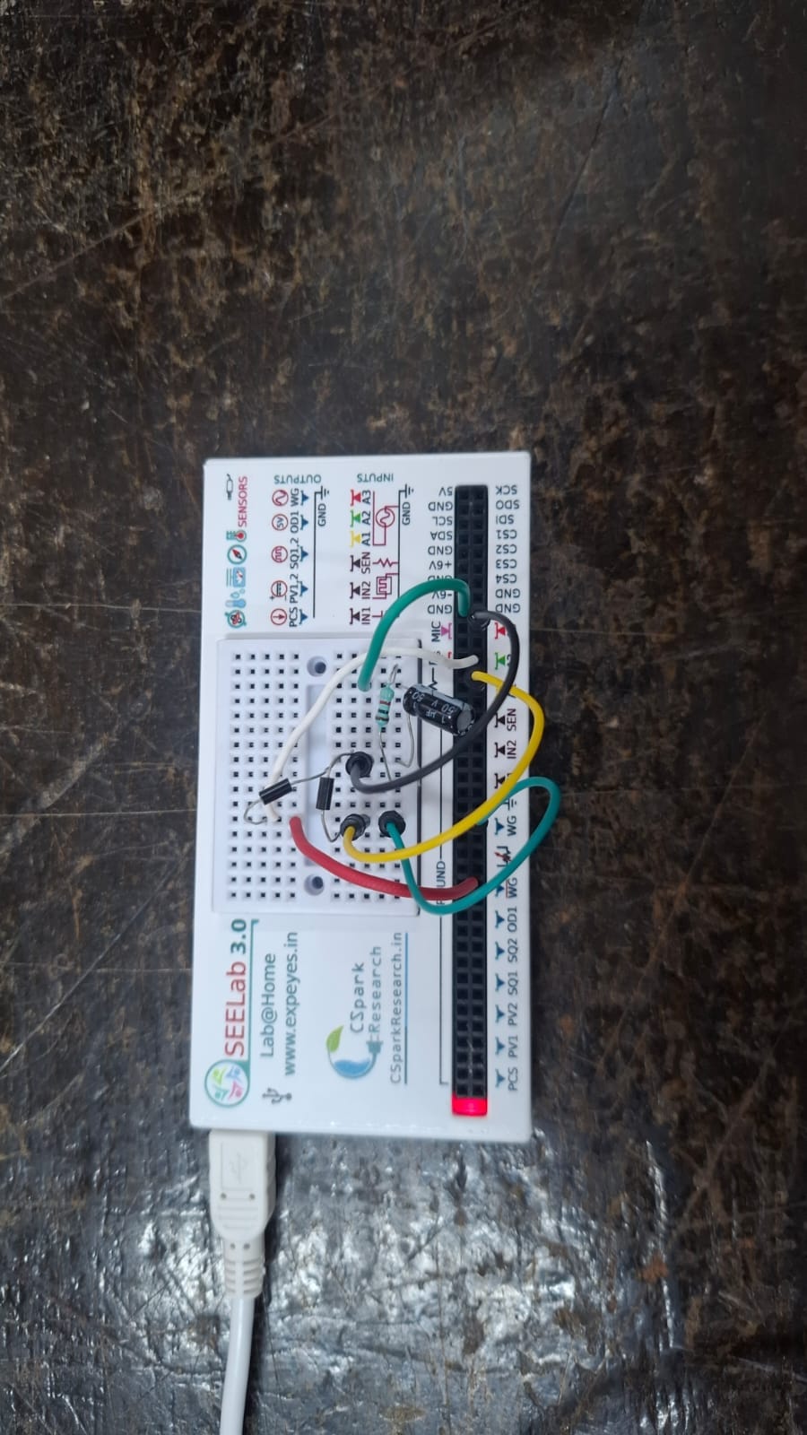
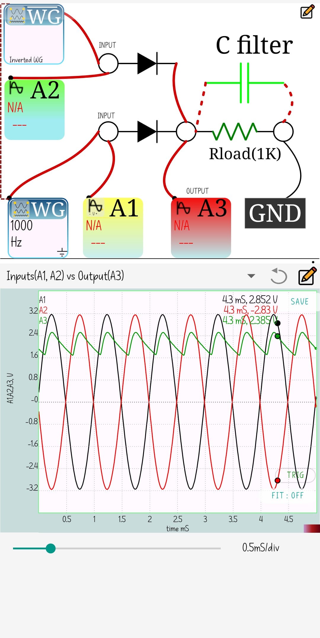
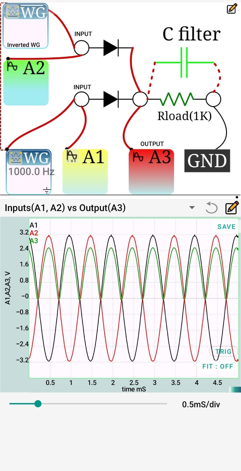
The setup uses SEELab3's WG and its inverted output as two 180°-out-of-phase sources, mimicking a center-tapped transformer secondary. Each feeds a diode, and both diodes join at a common output across a 1K load resistor, with a capacitor filter that can be switched in or out across the load.
Without the filter, A3 clearly shows a full-wave rectified waveform — two humps per input cycle, dropping to zero between them, since each diode conducts only for its own half-cycle. Adding the capacitor across the load smooths this into a waveform that stays mostly high, dipping by only about 0.8V as the capacitor discharges through Rload between conduction peaks. This is the classic effect of a reservoir capacitor: it charges to the peak voltage while a diode conducts, then holds the voltage up until the next diode fires.
Half-Wave Rectifier: With and Without a Filter
A single-diode half wave rectifier studied with SEELab3 — first without a filter capacitor, then with one added across the load, to see how the output waveform changes
Apparatus :SEELab3, breadboard, 1 diode, 1K load resistor, filter capacitor, jumper wires — using SEELab3's WG (1000 Hz) as the input source.
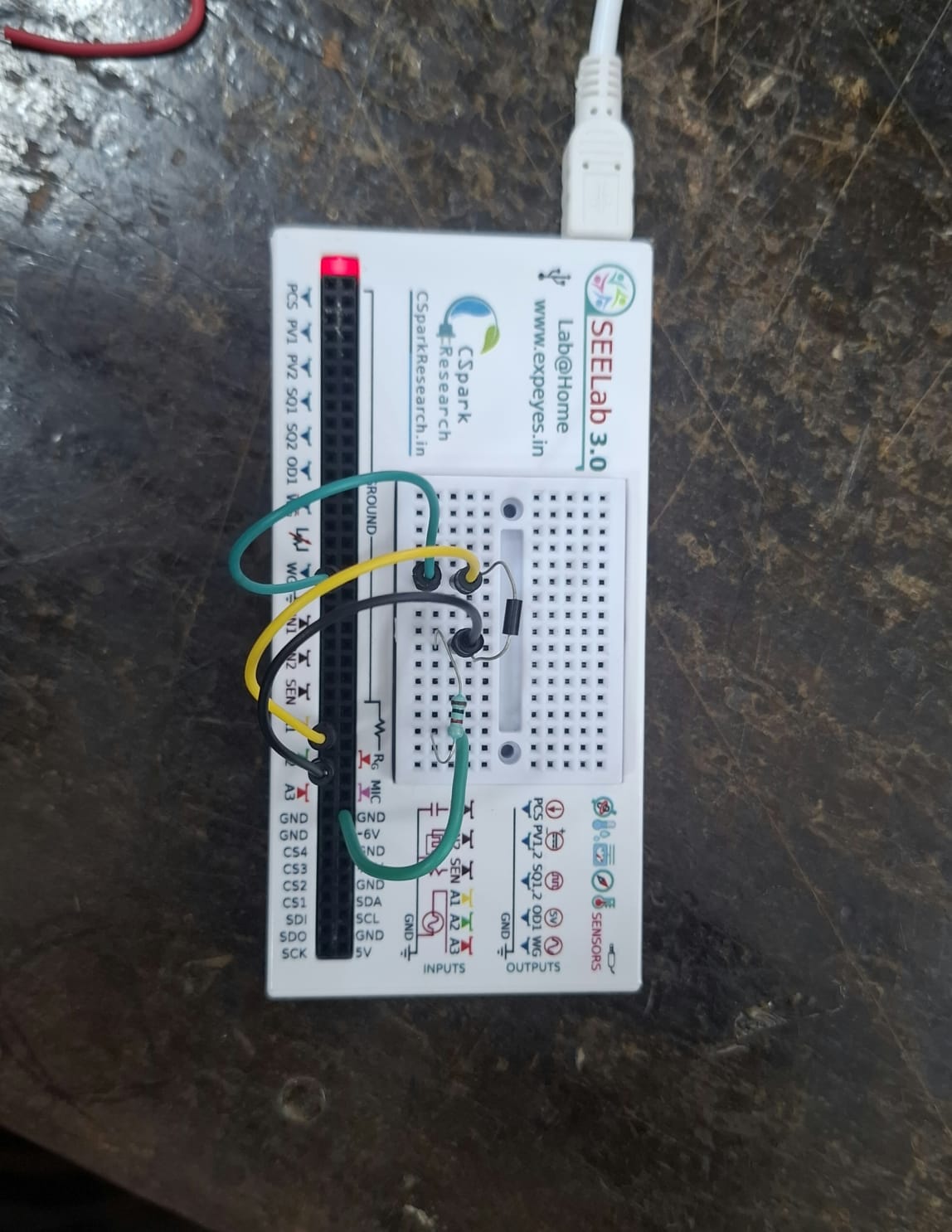
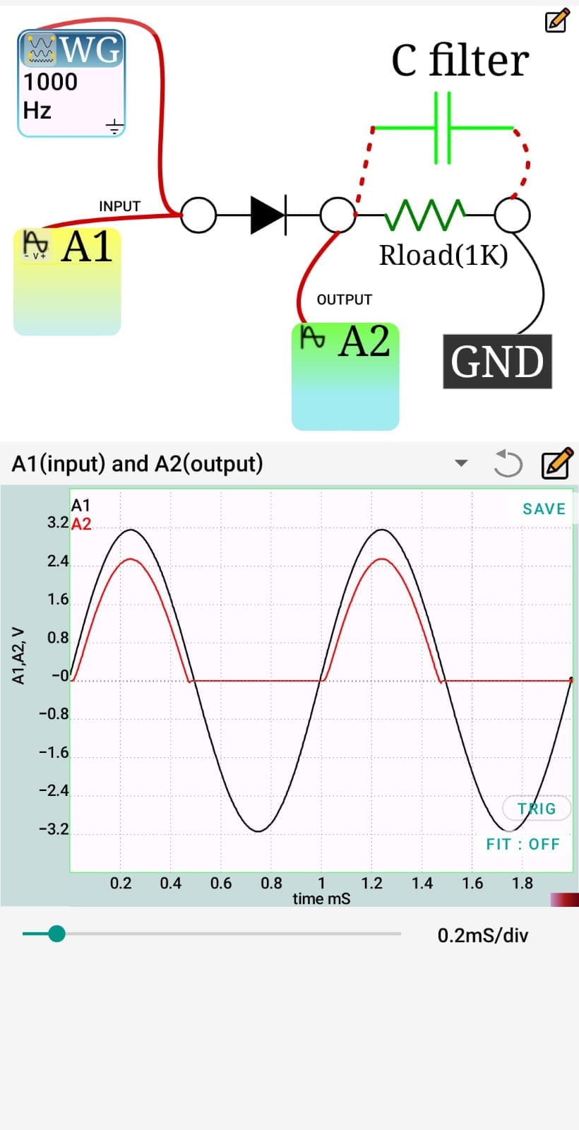
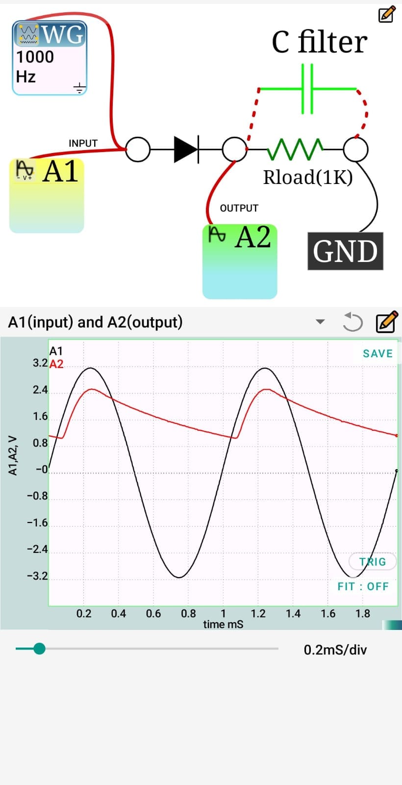
Observation : A single-diode half-wave rectifier was built with a 1K load, driven by the WG at 1000 Hz. Without the filter capacitor, output A2 followed only the positive half of each input cycle — tracking up to about 2.4V (below A1's 3.2V peak due to the diode's forward drop), then flattening at 0V for the entire negative half-cycle since the diode blocks reverse current. Adding the capacitor across the load changed this completely: A2 now charged up to the same ~2.4V peak during conduction, but instead of dropping to zero, it discharged slowly through Rload over the diode's off-half, producing a large ripple of about 1.6V. This ripple is much bigger than in the full-wave case, since here the capacitor has a full half-cycle to discharge instead of just a quarter — showing why full-wave rectification is generally preferred when smoother DC is needed.
RC Integrator
This experiment investigates the operation of an RC integrator circuit using the SEELab 3 (ExpEYES) platform. The circuit consists of a resistor and a capacitor connected in a configuration that produces an output voltage approximately proportional to the time integral of the input voltage. A square-wave signal is applied to the circuit, and the input and output waveforms are observed using the SEELab software.
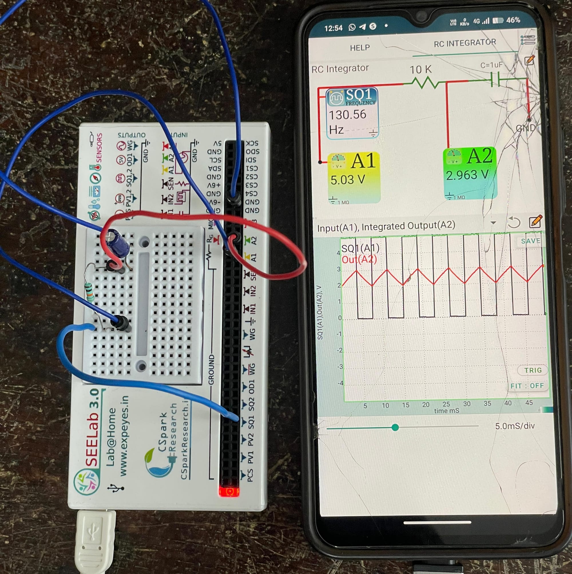
The experiment demonstrates the frequency-dependent behaviour of RC circuits and the principle of signal integration. When the circuit operates under suitable conditions, the square-wave input produces an approximately triangular output waveform. The experiment helps students understand the charging and discharging of capacitors and the practical applications of RC integrators in signal processing and electronic circuits.
𝗗𝗜𝗢𝗗𝗘 𝗖𝗟𝗜𝗣𝗣𝗜𝗡𝗚
The Diode Clipping experiment demonstrates how a diode limits the amplitude of an input signal by clipping portions of the waveform that exceed a specified voltage level. A sine-wave signal is applied to a clipping circuit, and a reference voltage (PV1) is used to set the clipping level. When the input voltage exceeds the reference voltage by approximately the diode's forward voltage drop (about 0.6–0.7 V for a silicon diode such as the 1N4148), the diode conducts and limits the output voltage.
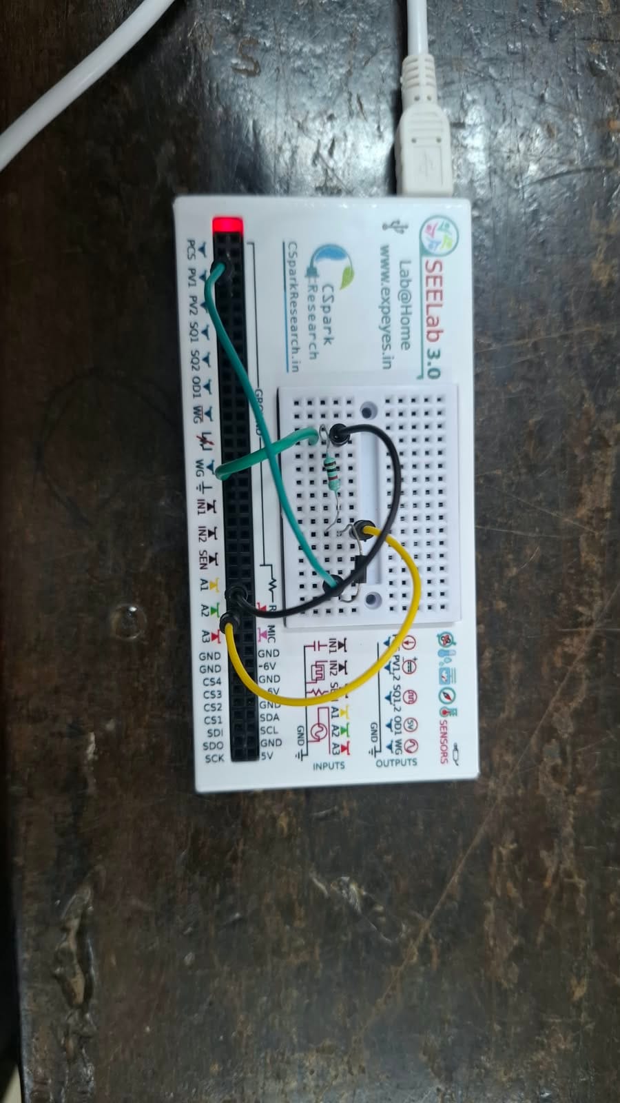
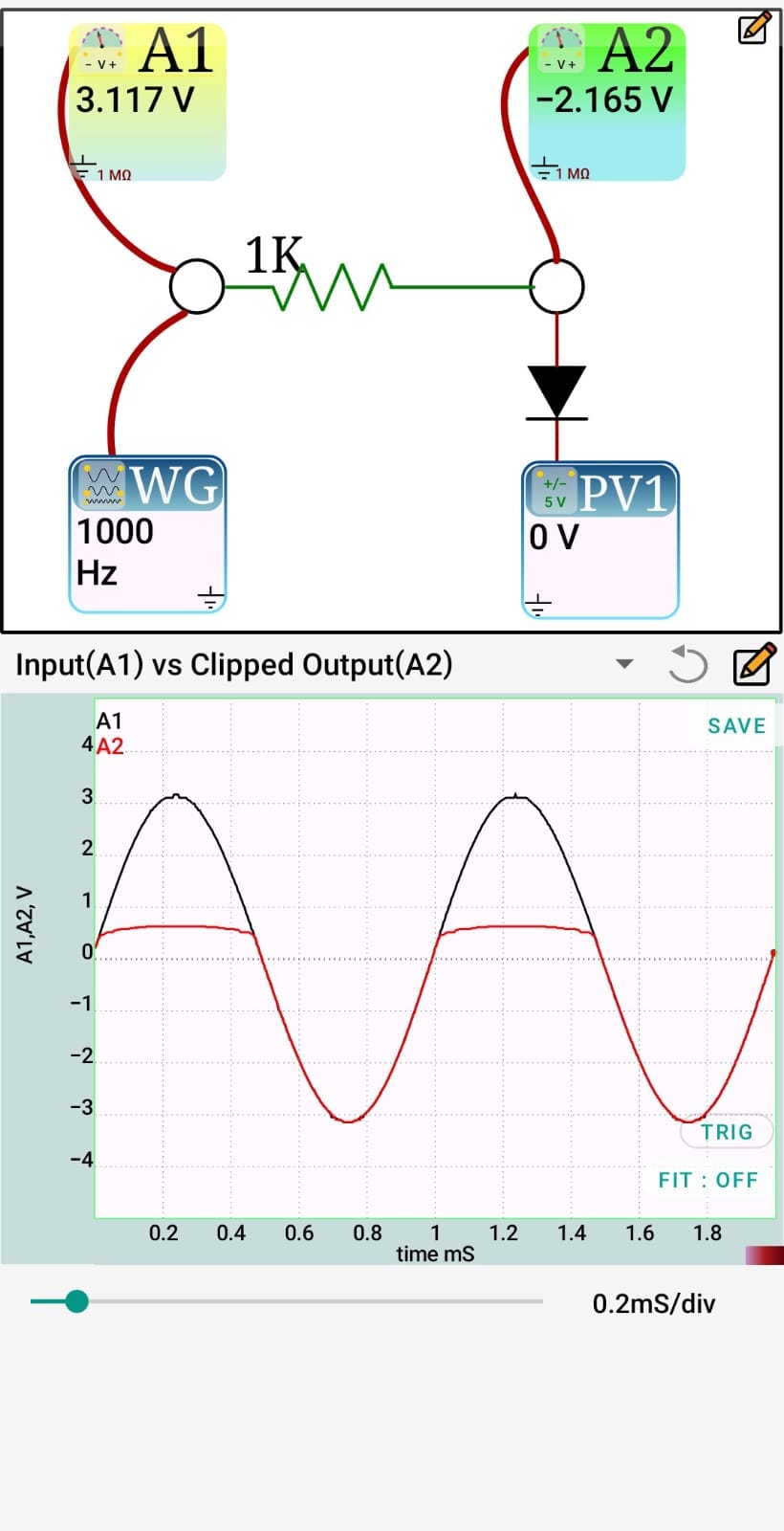
Using the SEELab 3 (ExpEYES) platform, the input and output waveforms can be observed and compared while varying the reference voltage. The experiment demonstrates the operating principle of diode clippers and their applications in waveform shaping, signal limiting, and electronic protection circuits.
Ohm's Law with Alternating Current
This experiment verifies Ohm's Law using alternating current (AC). A known 1 kΩ resistor and an unknown resistor are connected in series, and the RMS voltages are measured using ExpEYES/SEELab. The current is calculated from the voltage drop across the known resistor, allowing the unknown resistance to be determined.
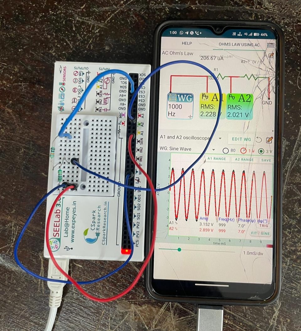
The experiment also introduces the concept of RMS (Root Mean Square) value, which represents the equivalent DC voltage or current that produces the same power as an AC signal. The measured results can be compared with the expected resistor values to verify Ohm's Law for AC circuits.
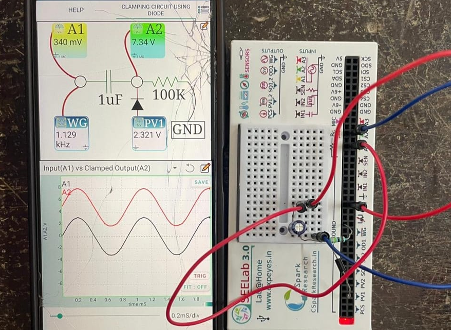
𝗗𝗜𝗢𝗗𝗘 𝗖𝗟𝗔𝗠𝗣𝗜𝗡𝗚 𝗘𝗫𝗣𝗘𝗥𝗜𝗠𝗘𝗡𝗧 The Diode Clamping experiment demonstrates how a diode and a DC voltage source can shift the average (DC) level of an AC signal without significantly changing its waveform shape. A sine wave from the waveform generator is applied to the clamping circuit, while the PV1 voltage source determines the reference level for the voltage shift.
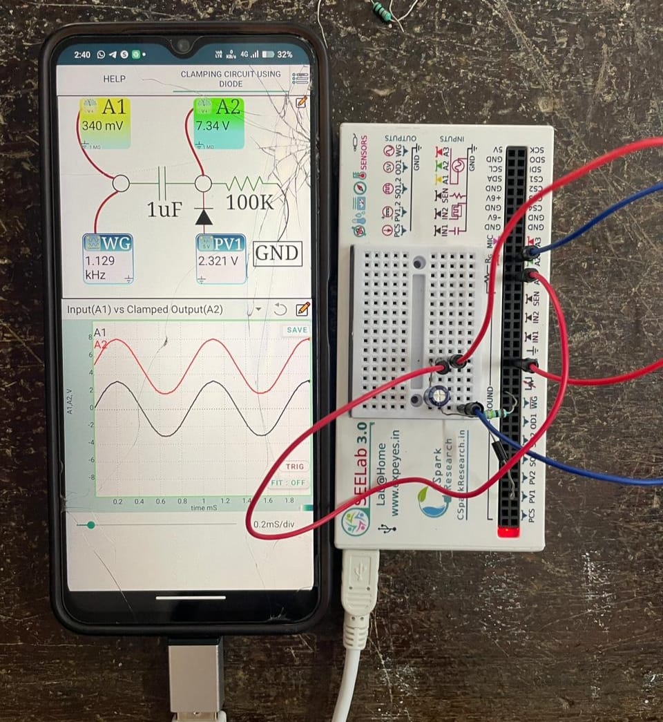
Using ExpEYES/SEELab, the input waveform is observed at A1 and the clamped output waveform at A2. By adjusting the PV1 voltage, the output waveform can be shifted upward or downward. The experiment illustrates the principle of diode clamping and its applications in DC level shifting and electronic signal processing.
𝗥𝗖 𝗦𝗧𝗘𝗔𝗗𝗬-𝗦𝗧𝗔𝗧𝗘 𝗥𝗘𝗦𝗣𝗢𝗡𝗦𝗘
An RC circuit consists of a resistor and a capacitor connected to an electrical source. When an AC signal is applied, the capacitor repeatedly charges and discharges, producing a response that depends on the resistance, capacitance and frequency of the input signal. After the initial transient effects disappear, the circuit reaches its steady state.
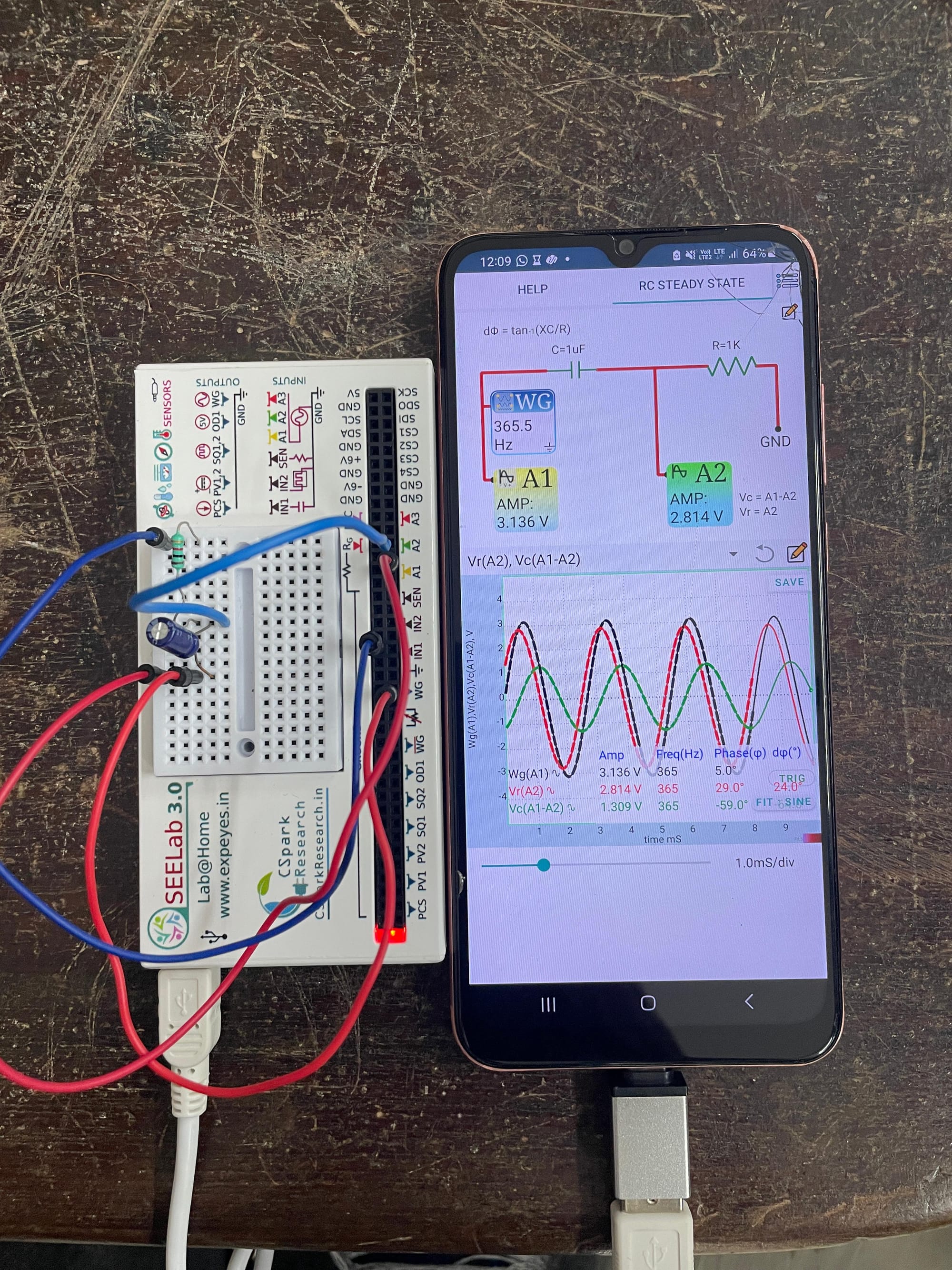
Using SEELab 3, the input and output signals can be observed to study the steady-state behaviour of the circuit. The experiment helps demonstrate the phase difference between voltage and current in capacitive circuits and the influence of the time constant RC on circuit response.
𝗥𝗟 𝗦𝗧𝗘𝗔𝗗𝗬-𝗦𝗧𝗔𝗧𝗘 𝗥𝗘𝗦𝗣𝗢𝗡𝗦𝗘
An RL circuit consists of a resistor and an inductor connected to an electrical source. When an AC signal is applied, the inductor opposes changes in current and produces a phase difference between the voltage and current. The steady-state response depends on the resistance, inductance and frequency of the applied signal.
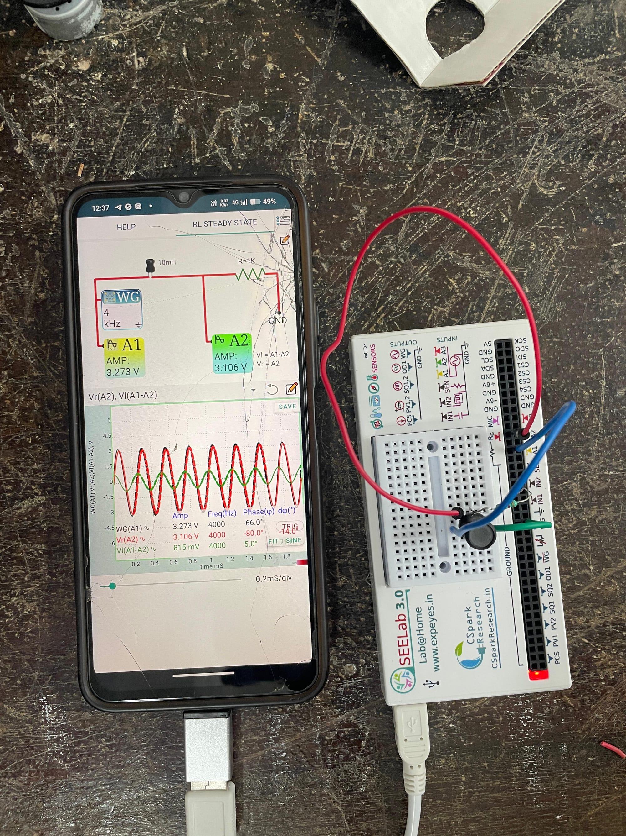
In this experiment, SEELab 3 is used to observe the electrical signals and examine the behaviour of the RL circuit after transient effects have disappeared. It helps explain inductive reactance, phase relationships and the role of inductors in AC circuits.
𝗔𝗡𝗗 𝗟𝗢𝗚𝗜𝗖 𝗚𝗔𝗧𝗘
An AND gate is a basic digital logic gate whose output is HIGH only when all its inputs are HIGH. For a two-input AND gate, the output is LOW when either input or both inputs are LOW. Its logical operation is expressed as Y=A.B, where A and B are the inputs and Y is the output.
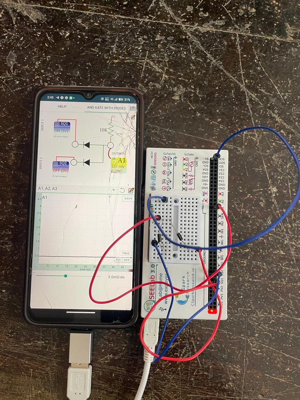
In this experiment, different combinations of input signals are applied and the corresponding output is observed using SEELab 3. The results can be compared with the truth table of the AND gate. This experiment introduces the fundamentals of digital electronics and the use of logic gates in digital circuits.
𝗭𝗘𝗡𝗘𝗥 𝗗𝗜𝗢𝗗𝗘 𝗩-𝗜𝗖𝗛𝗔𝗥𝗔𝗖𝗧𝗘𝗥𝗜𝗦𝗧𝗜𝗖𝗦
A Zener diode is a semiconductor diode designed to operate in the reverse-breakdown region under specified conditions. In forward bias, it behaves similarly to an ordinary diode. In reverse bias, the current remains relatively small until the breakdown region is reached, after which the current increases significantly while the voltage across the diode changes comparatively little.
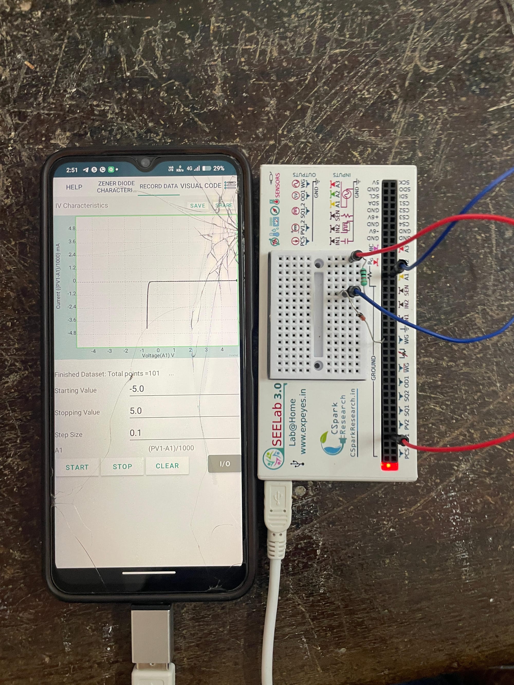
In this experiment, the voltage across the Zener diode and the current through it are measured under forward- and reverse-bias conditions. The V–I characteristic curve is plotted using the experimental observations. This helps explain Zener breakdown and the use of Zener diodes in voltage regulation and reference circuits.
𝗥𝗟 𝗧𝗥𝗔𝗡𝗦𝗜𝗘𝗡𝗧 𝗘𝗫𝗣𝗘𝗥𝗜𝗠𝗘𝗡𝗧 The RL transient experiment demonstrates how current changes in a circuit containing a resistor and an inductor when a DC voltage is switched on or off. Due to self-induction, the inductor opposes sudden changes in current, causing the current to rise or fall gradually rather than changing instantaneously.
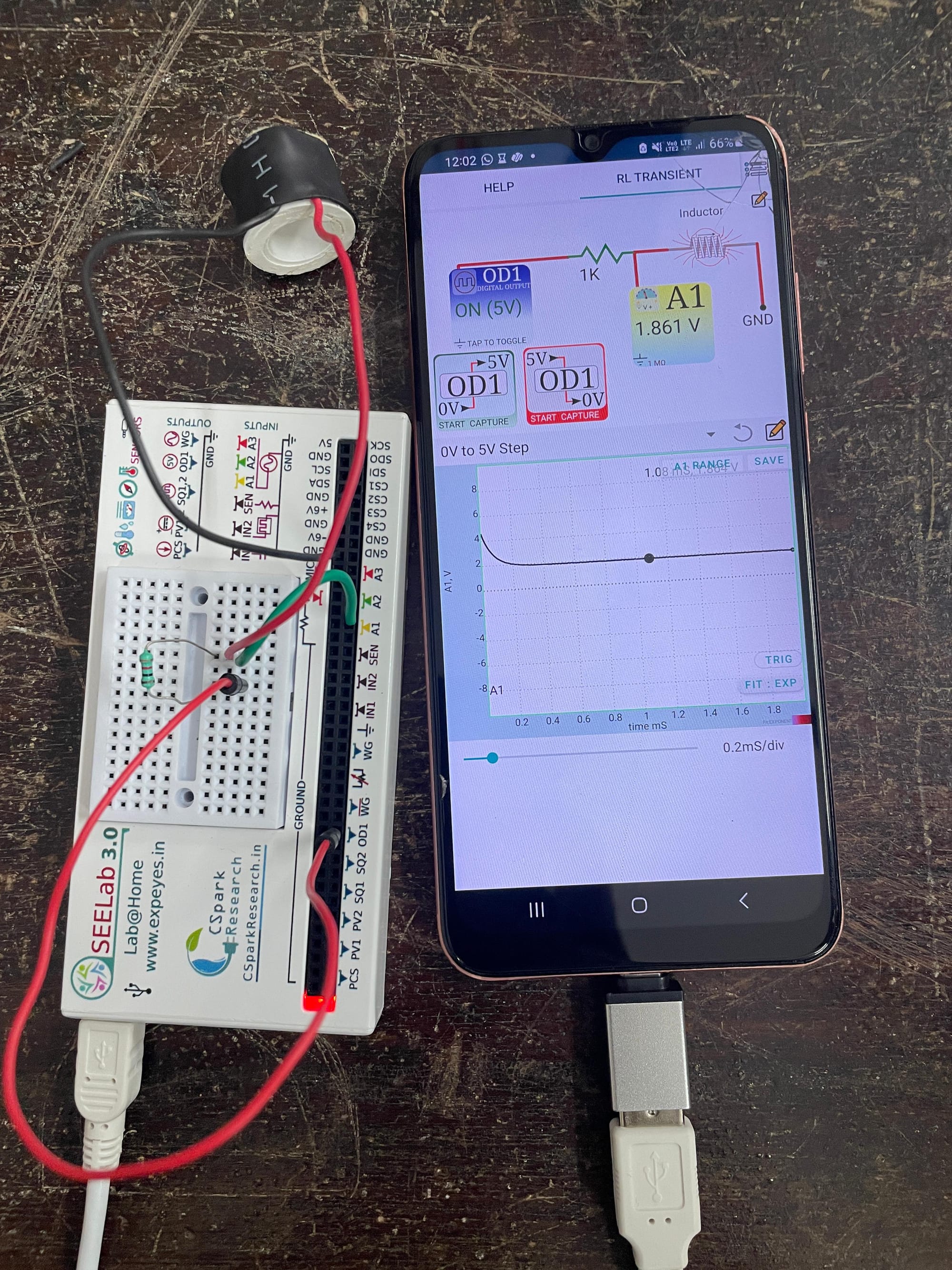
In this experiment, the transient response of the RL circuit is observed using SEELab 3. The time constant of the circuit depends on the inductance and resistance, given by (\tau = L/R). This experiment helps us understand the energy storage property of inductors and their behaviour during switching. 𝗥𝗟𝗖 𝗧𝗥𝗔𝗡𝗦𝗜𝗘𝗡𝗧 𝗥𝗘𝗦𝗣𝗢𝗡𝗦𝗘 𝗘𝗫𝗣𝗘𝗥𝗜𝗠𝗘𝗡𝗧 The RLC transient response experiment studies the behaviour of a circuit containing a resistor, inductor, and capacitor during transient conditions. When a voltage is applied or removed, energy is exchanged between the capacitor and inductor, while the resistor dissipates energy.
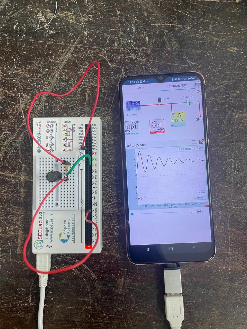
Using SEELab 3, the voltage response of the circuit can be observed over time. Depending on the circuit parameters, the response may be overdamped, underdamped, or critically damped. This experiment helps explain oscillations, damping, and energy transfer in electrical circuits. 𝗧𝗥𝗔𝗡𝗦𝗜𝗦𝗧𝗢𝗥 𝗔𝗠𝗣𝗟𝗜𝗙𝗜𝗘𝗥 𝗘𝗫𝗣𝗘𝗥𝗜𝗠𝗘𝗡𝗧 A transistor amplifier is used to increase the amplitude of a weak electrical signal. A small input signal controls a larger output signal, making the transistor an important component in audio systems, communication circuits, and electronic devices.
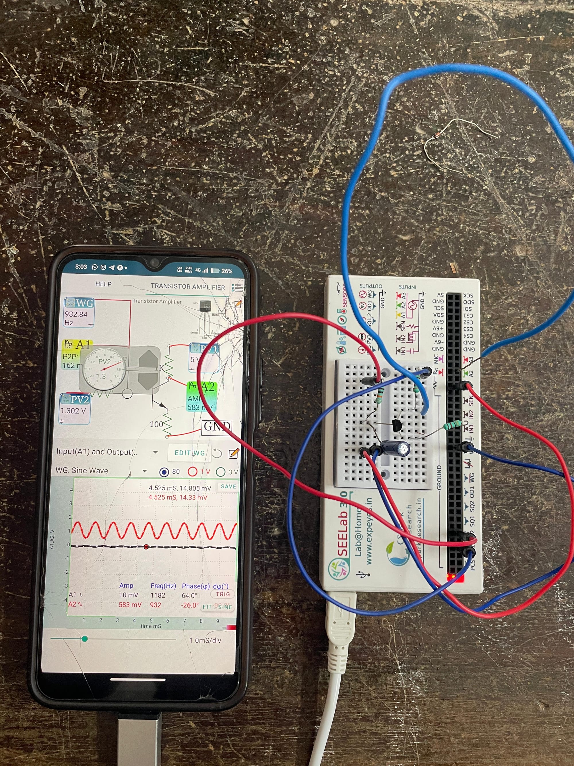
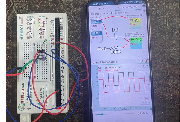
In this experiment, the input and output signals of a transistor amplifier are observed using SEELab 3. By comparing the signals, the amplification effect can be studied. The experiment helps demonstrate the role of transistors in signal amplification and the importance of biasing for proper amplifier operation. 𝗦𝗘𝗣𝗔𝗥𝗔𝗧𝗜𝗡𝗚 𝗔𝗖 𝗔𝗡𝗗 𝗗𝗖 𝗖𝗢𝗠𝗣𝗢𝗡𝗘𝗡𝗧𝗦 An electrical signal may contain both alternating current (AC) and direct current (DC) components. The AC component varies with time, while the DC component represents the constant or average level of the signal. Separating these components is useful in analysing electrical signals and understanding their characteristics.
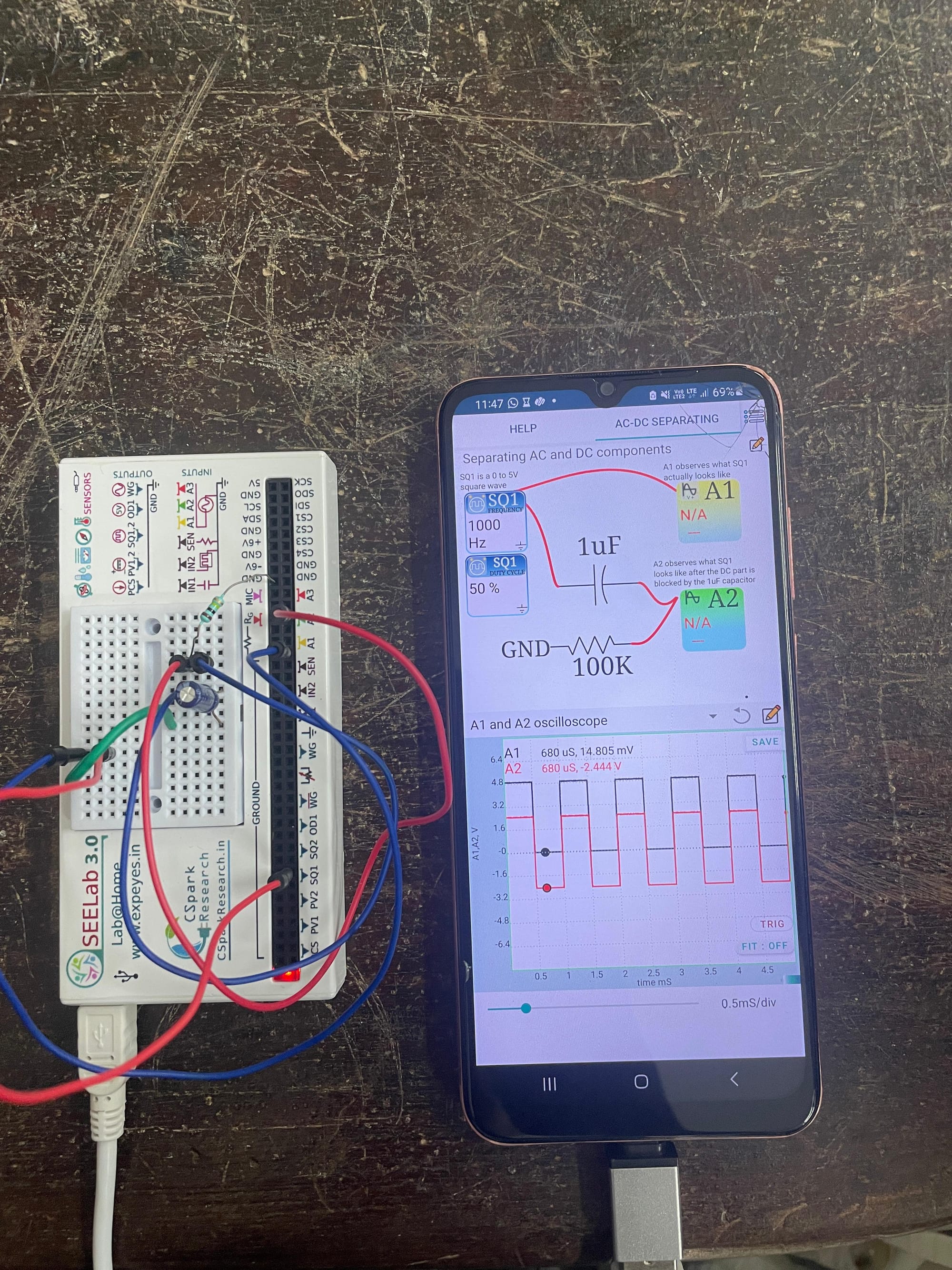
In this experiment, SEELab 3 is used to observe a signal and identify its AC and DC components. The DC component can be understood as the average value of the signal, while the AC component represents the variation around that average. This experiment provides a practical understanding of signal analysis in electronic circuits.